
Optical elements for photonic devices
With semiconductor technology becoming ever more powerful and pervasive, applications of semiconductor technology increasingly include optical functions. One example of optical elements for photonic devices is the increasing use of lasers and fibers in combination with integrated circuits for innovative sensing and communication applications.
Another example of how optical elements are used in photonic devices, is the emergence of microlenses to shape light from LEDs or lasers. These optical elements are often made in thin film technology, with benefits in quality, performance, reproducibility, size, and cost.
Optical elements ranging from EUV to IR
The Innovation Engineering MEMS foundry has been working with leading companies in the domain of integrating optical functions into photonic devices, providing thin film (MEMS) process development and manufacturing services. The following optical elements have been made for applications in the wavelength regime ranging from extreme ultra-violet (EUV) through infra-red (IR):
- Silicon Fresnel lenses (IR)
- Silicon and GaAs based microlenses (UV, IR)
- Fabry Pérot interferometers
- Optical coatings (anti-reflection, mirrors, filters)
- Gratings for outcoupling of light from solid state lasers
- Gratings for (F)IR sensors like spectrometers
- Spectral filters based on nanometer thick membranes
- Photonic crystals (various metals, shapes, and dimensions)
- Alignment markers on various substrates
Spectral filters can be made for wavelengths in the EUV-IR range, using various materials such as metals, metal silicide and silicon nitride and exhibiting dimensions from micrometers to 150 mm.
Interested in how we can add optical elements into your photonic devices? Contact our experts in optical elements for photonic devices ›
Optical elements for photonic devices in the spotlight

Artist’s impression of Sentinel-5p with the TROPOMI instrument on board. Credit: ESA
Innovation Engineering travels into space
For our customer SRON, the Netherlands Institute for Space Research, our MEMS Foundry contributed to the Sentinel5p project with a grating for IR-spectroscope on the Tropomi.
The Tropomi is the most advanced multispectral imaging spectrometer to date and is detecting worldwide air pollution.
Optical elements for photonic devices examples
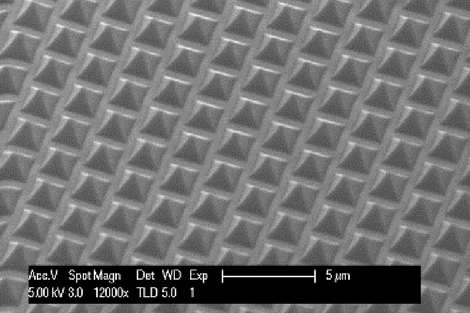
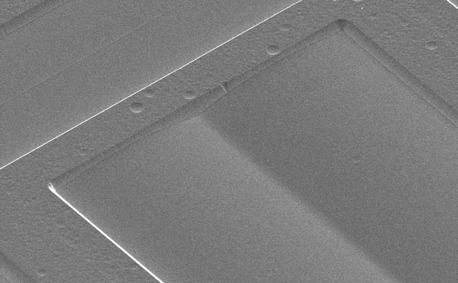
Pyramidal nanostructures
An example of SCIL (nano-imprint) based array with a base of 750 nm. Structures are imprinted in resist and dry etched on a silicon wafer.
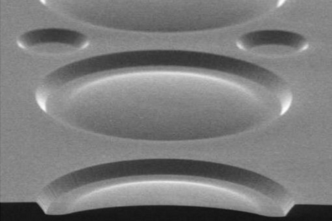
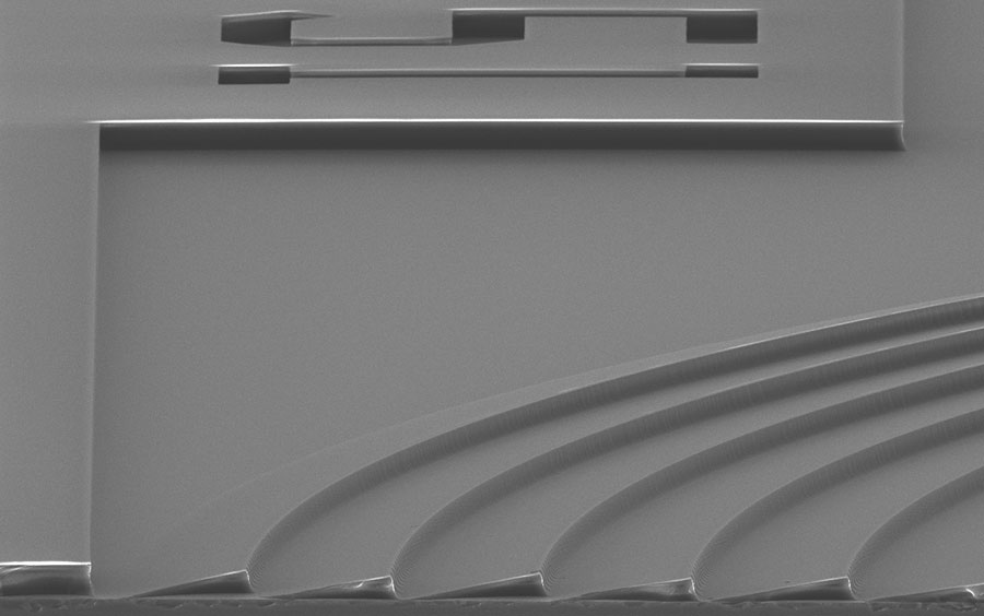
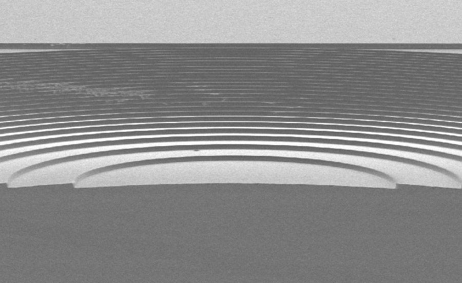
Wafer-based microlens
Wafer-based dry etched microlens for light out-coupling and collimation of solid state III-V lasers.
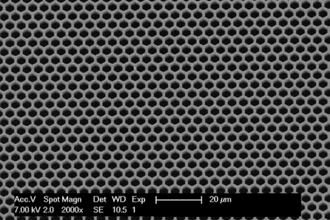
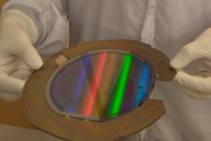
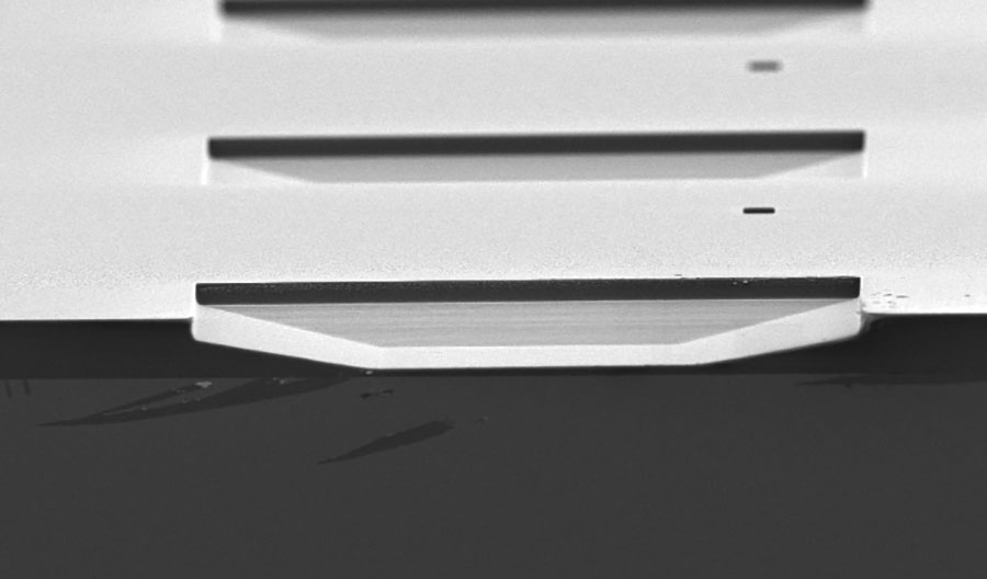
Perforated grid membrane
Made of a silicon wafer. The perforated membrane acts as a spectral filter for the EUV-IR range.
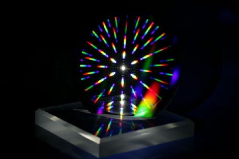
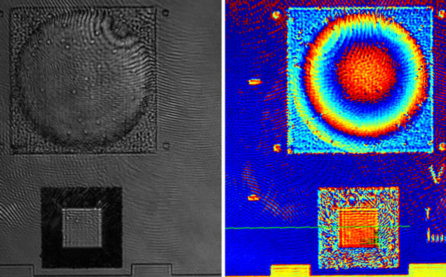
Grid membrane diffraction
Its honeycomb structure reveals a marvelous diffraction pattern when backlit with a white light point source.
Grayscale lithography
We offer silicon grayscale lithography as a manufacturable solution for a broad array of applications; from IR fresnel lenses, to lens arrays, gratings, concave mirrors to silicon and photonic connectors.
Our process is based on i-line stepper lithography on 200mm wafers and is compatible with all standard MEMS processing.
Specifications
- 0.5-20 µm deep features in silicon with 200 gray tones.
- 200 mm wafer process
- Maximum die sizes 22.0 mm x 27.4 mm
- Variable device feature densities and slopes/curves
- Local defined height and curvatures
Check out our other MEMS applications
MEMS applications are many. Organ-on-a-chip for example, where a human organ is reproduced in its most elementary form: microelectromechanical systems device. Several applications stand out, because of their promise and our capabilities.
Relevant for you: MEMS & Micro Devices 

Sustainable competitive advantage through custom MEMS devices. Check out our services in the MEMS & Micro Devices key area of expertise.